


Select UPWARDS partner institutions across the U.S. and Japan provided students with hands-on experience during a series of summer camps. These opportunities offered semiconductor education, industry engagement, cultural exchange, and research experiences, ultimately strengthening both technical skills and global collaboration.
Hiroshima University
July 22–August 2, 2026
Hiroshima University hosted the “UPWARDS Summer Intensive Program 2026: Peace and Semiconductor Innovation” as part of the “UPWARDS for the Future” initiative. The program was at Hiroshima University’s Higashi-Hiroshima Campus, particularly the Research Institute for Semiconductor Engineering (RISE). Off-campus activities included visits to Micron Memory Japan, Renesas Semiconductor Manufacturing Co., Ltd. (Saijo Factory), and Sumitomo Heavy Industries Material Solutions; Peace Study at Hiroshima Peace Memorial Park and the Hiroshima Peace Memorial Museum; an okonomiyaki-making experience; and a visit to the Shimanami Kaido.
In their own words:
- “In Hiroshima, we wanted students to learn not only how semiconductors are made, but also why we make them. Watching students from Japan and the U.S. design, fabricate, and measure devices together, and reflect together on the meaning of peace, was the greatest reward of this program. We look forward to welcoming the next generation of UPWARDS students.” — Professor Akinobu
- “Going to Hiroshima and learning about the bombing was the most valuable part. Getting to learn about history and connect it to your actions and what you want to do with your career is very important.” — Student, Purdue University
Rensselaer Polytechnic Institute (RPI)
August 2–15, 2026
At RPI, students were divided into three cohorts. Each cohort participated in learning modules in the following areas:
- Clean room: students learned the basic steps of deposition, lithography, etching, and metrology, resulting in a wafer with the UPWARDS logo. Students took the wafers home with them.
- Optics: students learned about Raman spectroscopy
- Computation: learned how to leverage machine learning to accelerate materials discovery for next-generation semiconductor materials and magnetic materials that enable advances in science and technology
- Semiconductor Devices: students took measurements of semiconductor devices; measured output currents and voltage
- Students also participated in a DEI exercise aimed at helping them examine different types of privilege.
The educational activities took place on our main campus in Troy, NY. Field trips included various locations in New York state: Saratoga Springs, Manhattan, Lake George and Albany.
By the Numbers: 17 total participants
- Tohoku University: 5 students
- Rensselaer Polytechnic Institute: 2 students
- Purdue University: 1 student
- Nagoya University: 2 students
- Institute of Science Tokyo: 3 students
- Hiroshima University: 2 students
- Kyushu University: 2 students
In their own words:
- “This program was a wonderful experience for me. Not only was the learning fantastic, but it was also a great opportunity to experience various aspects of American culture.” Visiting student
- “The program was highly effective, offering a rare and valuable combination of device physics, nano-fabrication, and data-driven materials informatics.”
Rochester Institute of Technology (RIT)
August 5–August 15, 2026
The UPWARDS Program at RIT provides students with a wide array of experience and exposure centered around hands-on-training sessions, technical demonstrations, tours of the Rochester Institute of Technology’s cutting-edge facilities and labs, time in clean rooms, seminars, and globally recognized company visits.
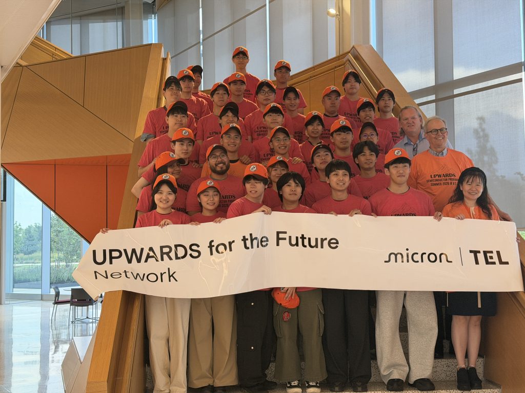
This summer, 22 students participated from five universities in Japan including: Nagoya University, Hiroshima University, Tohoku University, Institute of Science Tokyo and Kyushu University.
In addition to attending immersive campus seminars, students visited TEL (Tokyo Electron) in Albany, New York. Students were able to tour the facility and learn about the innovations and advancement in the semiconductor industry. Students also had the opportunity to participate in a panel that featured individuals from NY Creates and engineers and practitioners in the field.
Along with having the opportunity to explore the city of Rochester and enjoy its diverse culture, students also visited Niagara Falls and rode the Maid of the Mist boat tour.
In their own words:
- “I really enjoyed the visit to TEL. I was amazed to see such a large cleanroom and the advanced systems used to transport materials. It was a very interesting and memorable experience!” — Visiting student
- “I liked that the sessions covered both the fundamentals of semiconductor technology and its practical applications. They helped me better understand how academic research connects to industry.” — Visiting student
Virginia Tech (Virginia Polytechnic Institute and State University)
Session 1: July 20–31, 2026
Session 2: August 3–14, 2026
UPWARDS TechTrek at Virginia Tech was a hands-on, project-based STEM camp offered in two two-week sessions. Students explored artificial intelligence and machine learning, electronic circuits and memory, digital design and FPGAs, robotic cars and drone technology. Each session included 10 class days over two weeks.
Short lectures were paired with laboratories in Python programming, image classification, gesture recognition, sensing, logic, Arduino and Raspberry Pi hardware, robot assembly, line following, and navigation. Representative projects included maze-escape and line- tracking robots, robotic-dog gesture control, FPGA games and reaction testers, sign- language and facial-expression recognition, SRAM circuits, and autonomous drone or smart-car systems.
Students finished with team capstone projects that required planning, building, testing, debugging, documenting, and presenting. They gained technical foundations across the semiconductor and computing stack, practical laboratory experience, teamwork, communication, and presentation skills. College and career sessions also covered admissions, technical careers, entrepreneurship and intellectual property, energy and AI, research, publishing, and work-based learning.
By the Numbers:
- 90 high-school students: 46 in July and 44 in August
- Rising students in 10th, 11th and 12th grade
- Approximately 70 IEEE Semiconductor Leadership Certificates issued and
registered - Approximately 20 capstone teams: about 11 in July and 9 in August
- Daily feedback surveys and an end-of-program survey measured changes in STEM
interest and confidence
In their own words:
- “Thank you so much for everything, from handling travel arrangements to the program. This was a very valuable experience.”
Boise State University
A total of 12 Boise State University students participated in summer camps hosted by the following universities (two Boise State students per location):
- Kyushu University
- Hiroshima University
- Tohoku University
- Nagoya University
- Institute of Science Tokyo
- Virginia Tech
Student majors included Electrical and Computer Engineering, Materials Science Engineering, Mechanical Engineering and Computer Science. Because of the summer camp opportunities, multiple students also had the opportunity to travel around Japan after the programs because of these opportunities.
Feedback:
- “This has been a once in a lifetime experience and I am so grateful it happened!” — BSU Student
University of Washington (UW)
July 28–August 1, 2026
Attendees of the UW UPWARDS summer camp gained hands-on experience in semiconductor manufacturing and nanofabrication technologies through lectures and hands-on lab experience guided by UW UPWARDS faculty members. Interactive lecture courses in lithography, etch, deposition, metrology and troubleshooting were paired with the following labs:
- Wet Bench/Oxidize Wafers
- Lithography and Oxide Etch
- Lithography/Load Evaporator
- Liftoff and backside metal
- Measure and Test
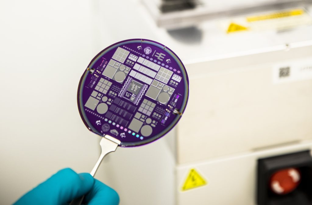
Students began the course with no cleanroom experience and finished the week confident in cleanroom protocols and with a solid understanding of the fabrication processes they performed and why they mattered. The students used the fabrication techniques they learned in lecture to fabricate their own devices-resistors, capacitors and Schottky diodes. The program concluded with students testing their wafers and taking them home.
In their own words
- “It was great! I feel lucky to have been selected for this.” — UW Student
- “It was well organized and time was well managed.” — UW Student
UW participation in UPWARDS partner summer camps: In addition to the camp offered on-campus in Seattle, Washington, eight UW students attended the following summer camps at partner universities in Japan:
- Tohoku University
- Hiroshima University
- Nagoya University
- Science Tokyo University
- Hiroshima University
- Science Tokyo University
- Kyushu University
- Nagoya University